- Joined
- May 23, 2008
- Messages
- 2,673
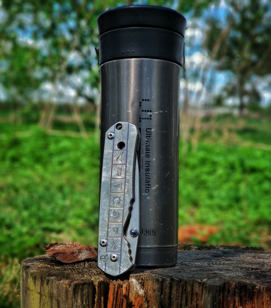
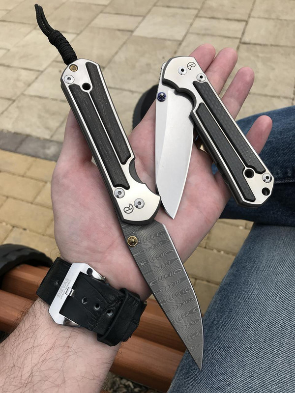
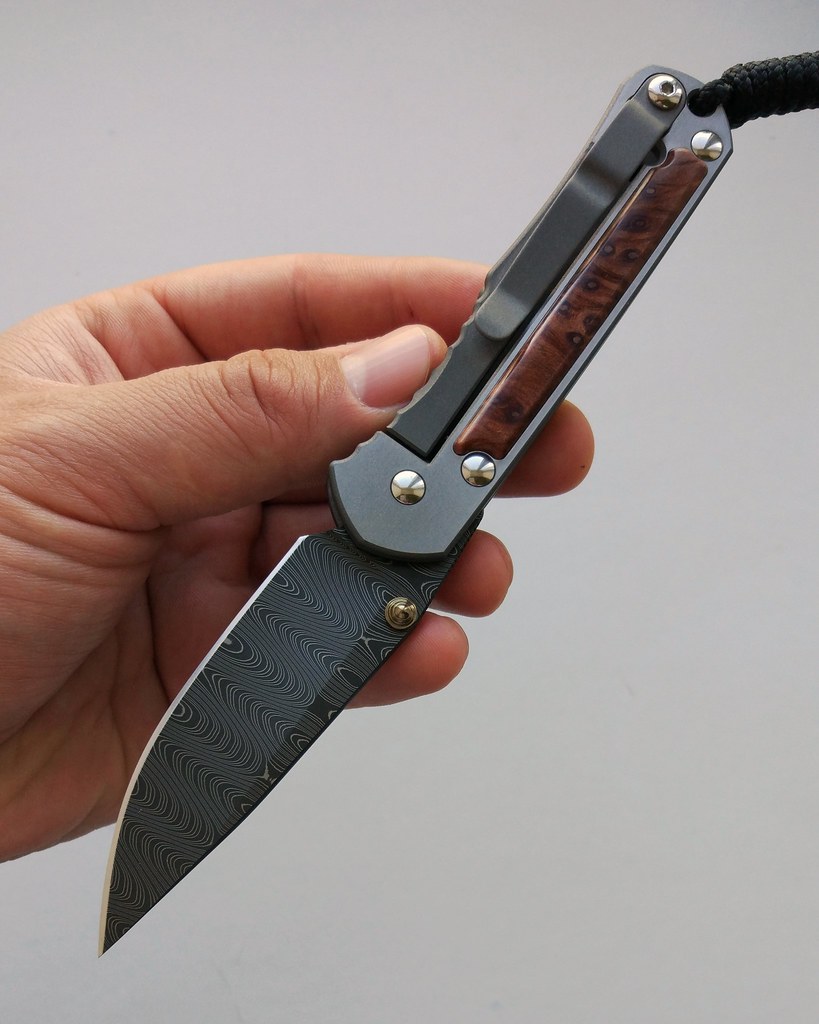
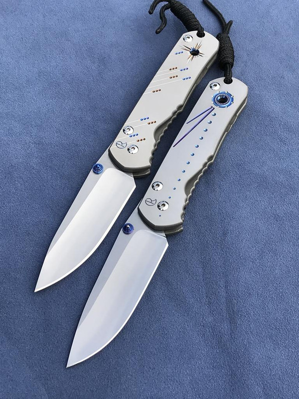
Snapped a few...


The BladeForums.com 2024 Traditional Knife is available! Price is $250 ea (shipped within CONUS).
Order here: https://www.bladeforums.com/help/2024-traditional/